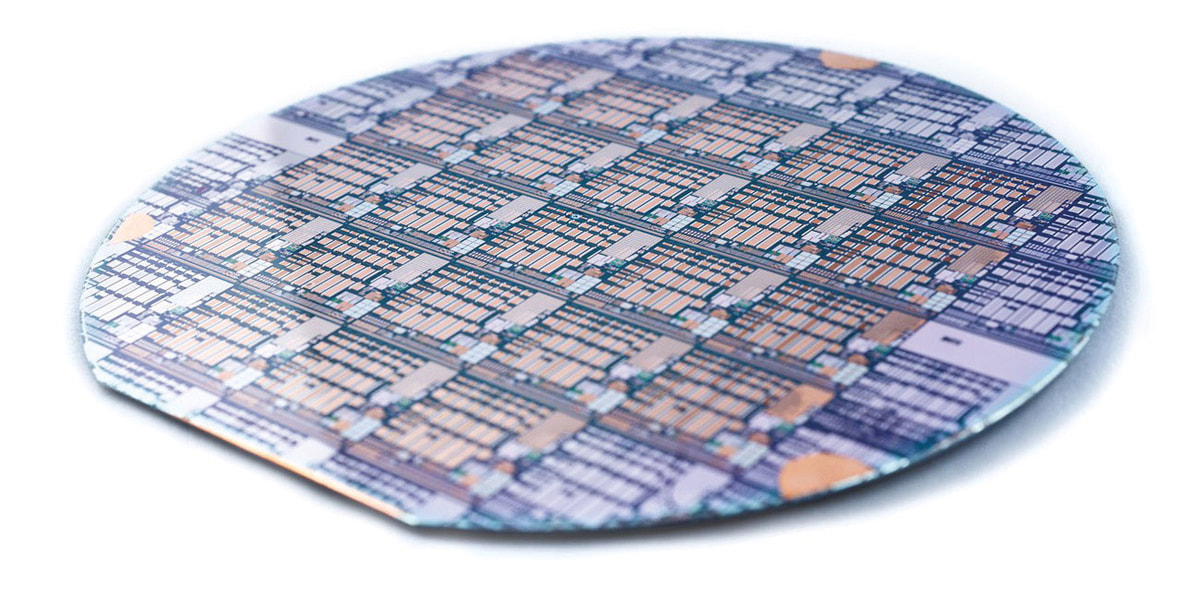
 GaN (gallium nitride) wafers, which are frequently used in laser, LED, and transistor products, are made from really bulk material and created using an advanced ammonothermal technique. The creation of non-polar M-plane, A-plane, and semi-polar Gan Epitaxial Wafers, as well as high quality bulk c-plane GaN substrates up to 2-inches in diameter, is the consequence of technological advancements in growing technology. These substrates are designed to be used in the fabrication of high electron mobility transistors, green and blue lasers, and light emitting diodes (LEDs) (HEMTs). Read More- https://www.gatorledger.com/expanding-semiconductor-industry-to-augment-demand-for-gan-epitaxial-wafers/
0 Comments
Leave a Reply. |
Categories
All
|
 RSS Feed
